Australian National Fabrication Facility – Griffith University Node (ANFF-Q)
Australian National Fabrication Facility
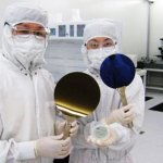
The Australian National Fabrication Facility (ANFF) Queensland Node provides researchers and industry with open access to semiconductor fabrication, processing and characterisation capabilities through the Queensland Microtechnology Facility (QMF) at Griffith University.
The Griffith University facility specialises in semiconductor and microfabrication technologies, with particular expertise in silicon carbide (SiC) and compound semiconductors. ANFF supports research and development of microelectronic and power electronic devices, as well as applications in photonics, quantum technologies, sensors, MEMS and microfluidics.
Through QMF, ANFF provides comprehensive cleanroom infrastructure supporting a broad range of micro- and nanofabrication processes, including photolithography, plasma etching, thin-film deposition, thermal processing, wet chemical processing, wafer cleaning, wafer dicing, and materials and device characterisation.
- Website
- https://anff-q.org.au/
- Organisation type
-
- National Collaborative Research Infrastructure Scheme facility
- Not-for-profit
- Number of research staff
- Up to 20 research staff
- Address
- QMF building (N74 Room 1.04), Griffith University, West Creek Road, Nathan QLD 4111
Strengths and capabilities
- Silicon carbide power device fabrication
- Epitaxial growth of 4H-SiC and 3C-SiC
- Compound semiconductor processing
- Photolithography
- Plasma etching
- Thin-film deposition
- Thermal processing
- Wet chemical processing
- Materials and device characterisation
- Electron and scanning probe microscopy
- MEMS and sensor fabrication
Facilities and major equipment
SiC epitaxy
- 4H-SiC epitaxial reactor
- 3C-SiC epitaxial furnace
Lithography
- Contact mask aligner
- Maskless laser writer
- Coater and developer
- HMDS vapour priming oven
- Hotplates
Plasma etching and processing
- Inductively coupled plasma (ICP) etchers
- Plasma ashing
Thin-film deposition
- Magnetron sputtering
- Electron-beam evaporation
- ICPCVD for oxides, nitrides and carbides
- LPCVD for low-temperature oxide and polysilicon
Thermal processing
- Wet and dry thermal oxidation furnaces
- Rapid thermal annealing
- Annealing and diffusion doping furnace
Wet processing
- Bench
- Single-wafer spinner for wet etching and cleaning
- Automated metal lift-off system
Laser micromachining
- Femtosecond laser CNC system
Microscopy and characterisation
- Scanning electron microscopy (SEM)
- Atomic force microscopy (AFM)
- Ellipsometry mapping
- Fourier-transform infrared (FTIR) spectroscopy and thickness mapping
- Optical microscopy
Electrical test laboratory
- Electrical and semiconductor device testing
Key science sectors
More information about the sectors this centre is involved in:
Update details
Is this your centre? See any issues? Send a request to update your listing.